A client provided four aluminum electrolytic capacitors to SEM Lab, Inc. for analysis. These were identified as counterfeit by the manufacturer that also examined some of the counterfeit capacitors.

Fig. A – Rubber seal styles for capacitor samples
There were a variety of construction anomalies associated with these samples. These are listed below by sample.
Sample A – Poorly constructed roll where lead spacing appeared to be bad and close proximity of swage to end of anode foil extremely unusual, as well as proximity of anode & cathode terminations. 5-swage terminations.
Sample B – same as A (except 3-swage terminations)
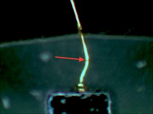
Sample C – 4-swage terminations, position of lead attachment on roll more typical than A or B where attachment was near start of roll. Corrosion damage in beginning stage on anode lead. Seal appears poor and damaged by stave on lead.
Sample D – 5-swage terminations, position of lead attachment on roll more typical than A or B where attachment was near start of roll. Corrosion damage in beginning stage on anode lead. Seal appears poor and damaged by stave on lead. D foil appears different than C foil.

Fig. B – Sample A – failed capacitor #1. This is the EDS spectrum of corrosion product on the anode near the corroded termination.
The analysis results suggest that the two failed samples became open-circuited due to internal corrosion at the anode lead. These failures may have been accelerated by poor quality seals and construction features that permitted ingress of external contamination (e.g. Cl) and moisture. The not-yet-failed samples also showed initial stages of corrosion failure at the anode lead/seal.
—