BGA Failure Analysis
Ball Grid Array (BGA) Failure Analysis
BGA failure analysis is made difficult by the high density of I/O pins in the Ball Grid Array (BGA) devices. BGA packaging involves the packing of large numbers, sometimes upwards of 400 to 500 I/O pins, into a relatively small area, which is their primary advantage to manufacturers. The high number of pins is also what makes the BGA failure analysis task so complex. Most BGA root cause failure analysis done at SEM Lab, Inc. has been related to warpage issues, black-pad-syndrome, brittle interfacial fracture, and assembly level process issues.
Examples of Scanning Electron Microscopy (SEM) images of BGA failures, BGA cross-sections and other failures seen in BGAs are shown below.
A paper describing BGA failure mechanisms we have seen at SEM Lab, Inc. can be found here.
Other device failure analysis information:
bga Failure Analysis
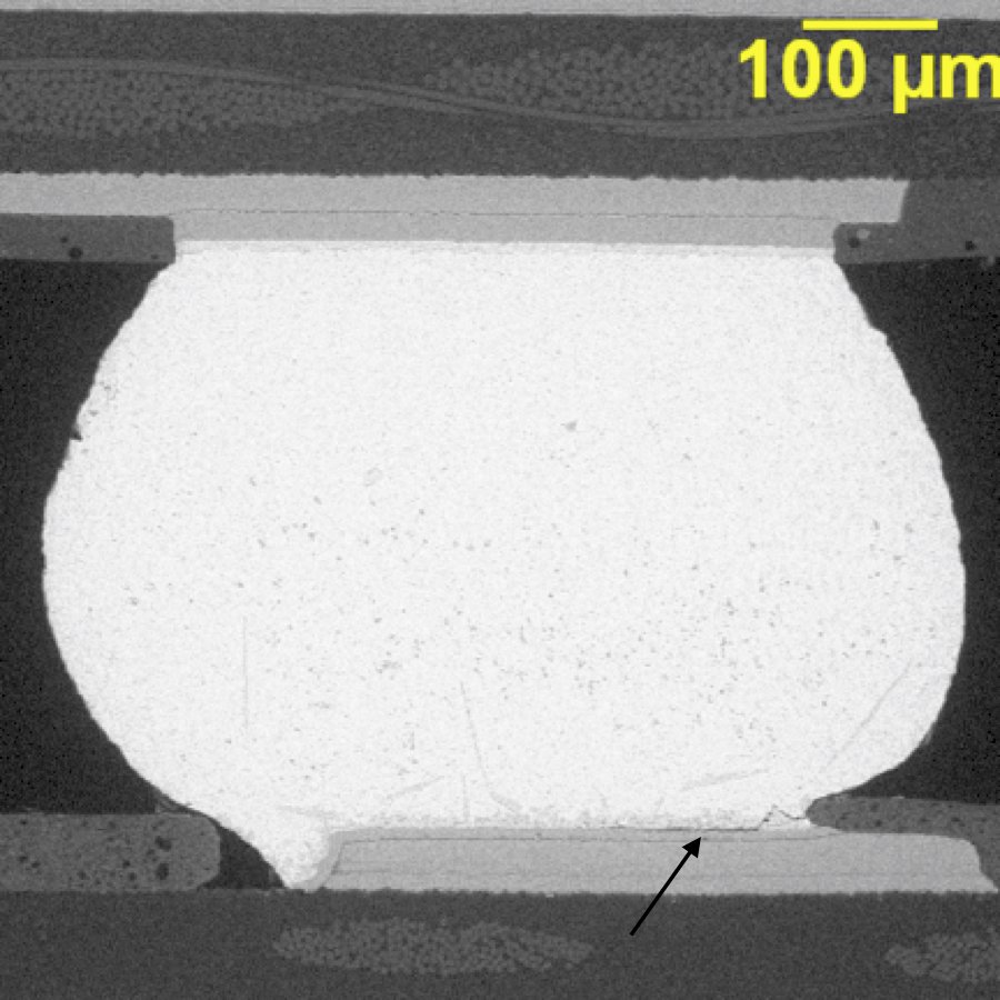
Ball Grid Array (BGA) solder joint.
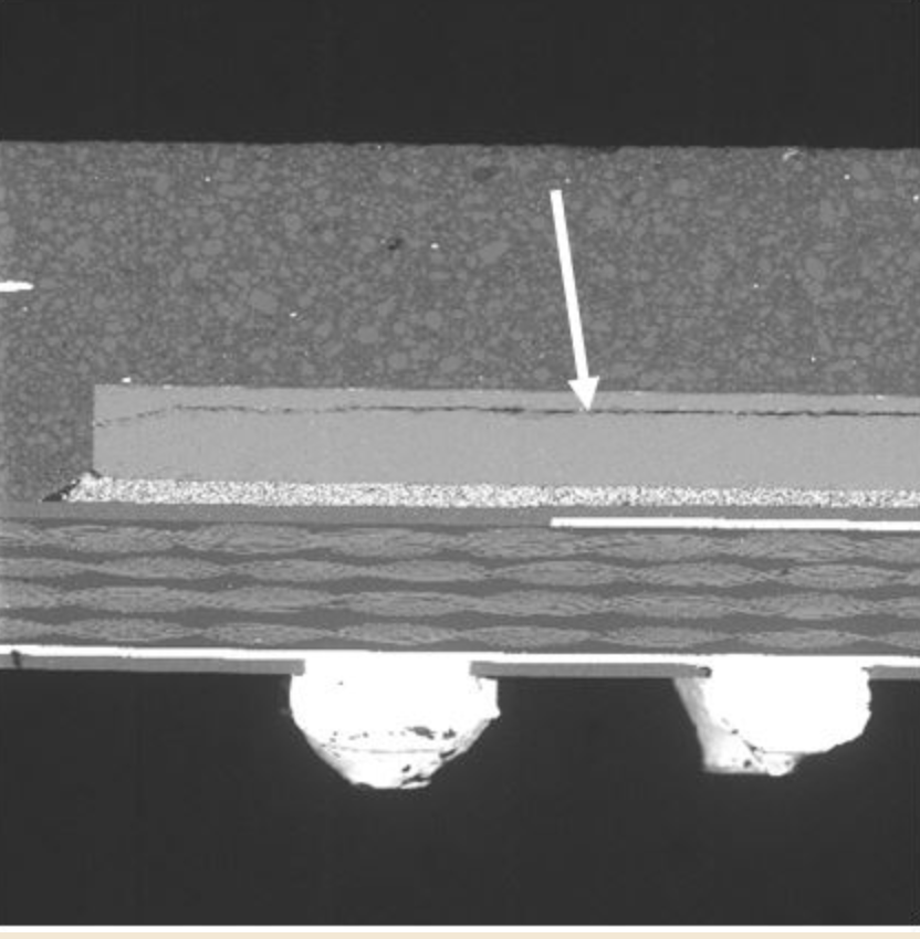
Warpage induced die crack on BGA.
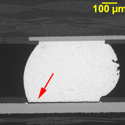
BGA solder joint fracture.
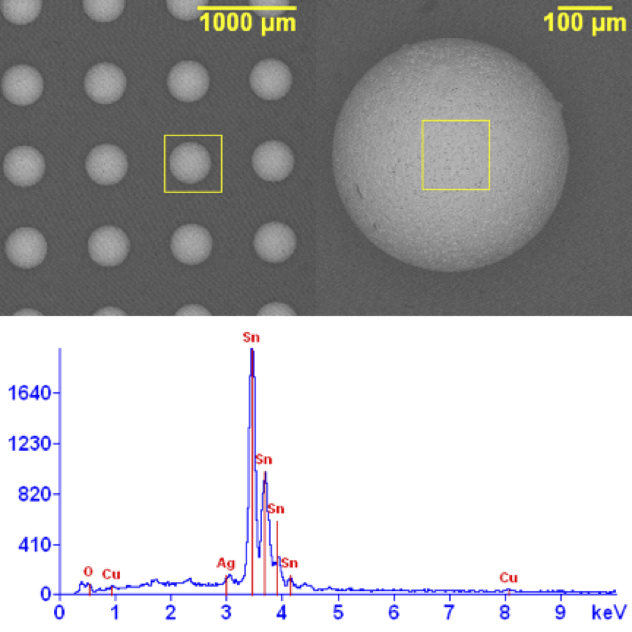
Solder ball composition.