Measuring Plating Thickness
Plating used on electrical component leads and as printed-wiring-board finishes is usually thin, less than 300 micro-inches, and it is important to verify that the plating thickness meets specifications. Consistent plating thickness is necessary to ensure proper performance during assembly. SEM Lab, Inc. has developed a method for measuring thickness of thin film deposits on various substrates, including multiple layers of different materials, using EDS data. The method is extremely efficient and is therefore a cost effect alternative to conventional and FIB microsection techniques (approximately half the cost).
Thickness Measurements for Optical Coatings
An accurate, efficient, and inexpensive approach to verification of thin film layer thickness
By using a SEM image and an EDS spectrum, SEM Lab, Inc. can calculate the thickness of the thin film layers, the condition of the surface and/or if any foreign contamination is present.
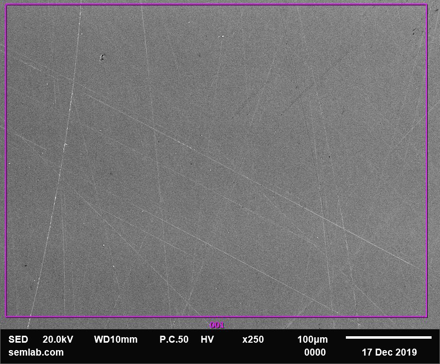
As an example, the SE SEM image of Au-Ni-Cr on Ge is shown below. Scratches can be seen on the optical surface.
The EDS spectrum of the sample, shown below, provides the basis for the thickness measurements.
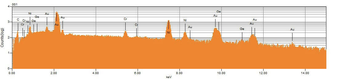
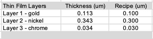
Using a proprietary algorithm the EDS spectrum is analyzed and the following thickness values are calculated. The results are compared to the recipe, showing very accurate results.
SEM/EDS analysis of coatings provides:
- the condition of the optical surface
- indicates if foreign contamination or oxidation is present
- provides accurate determination of thin film layer thickness
- very efficient compared to other measurement methods (e.g. FIB or standard microsections with SEM imaging)
ENIG Evaluation Using SEM/EDS Analysis
An accurate, efficient, and inexpensive approach to measuring gold thickness and phosphorous content in electroless nickel deposit gold thickness and phosphorous content in electroless nickel deposit
Gold plating thickness over nickel or nickel-phosphorus alloy can also be determined by SEM Lab, Inc. using this method. The thickness of the gold layer can be acquired for electroless-nickel immersion-gold (ENIG) PWB finishes and thin electro-plated gold (< 15 microns) on boards or component leads.
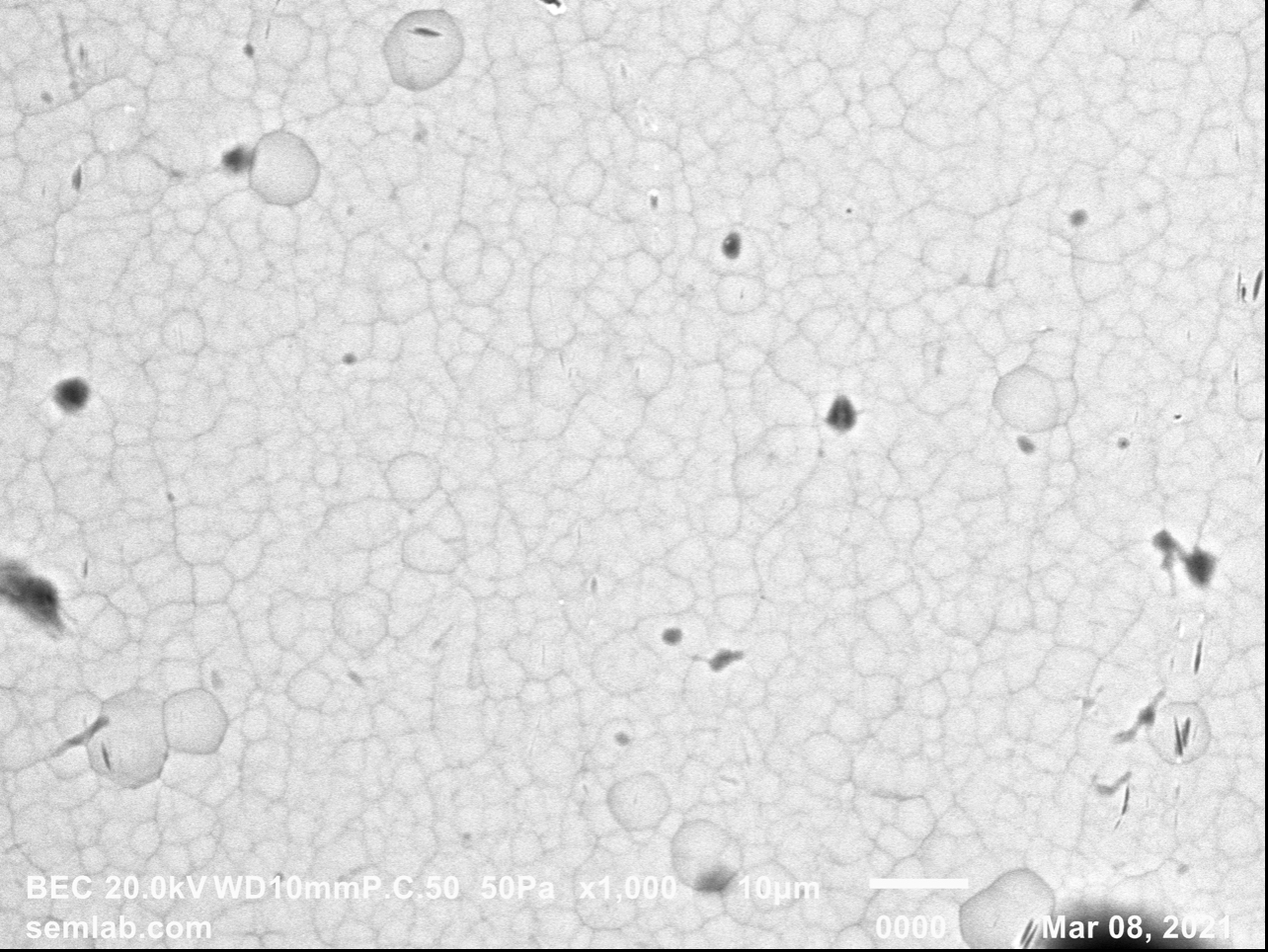
Shown below is a 1000X reference image of ENIG surface shows grain size, contamination, and evidence of grain boundary etching.
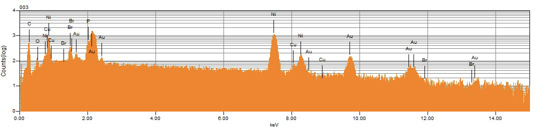
The EDS spectra of the sample identifies elemental constituents of contamination.


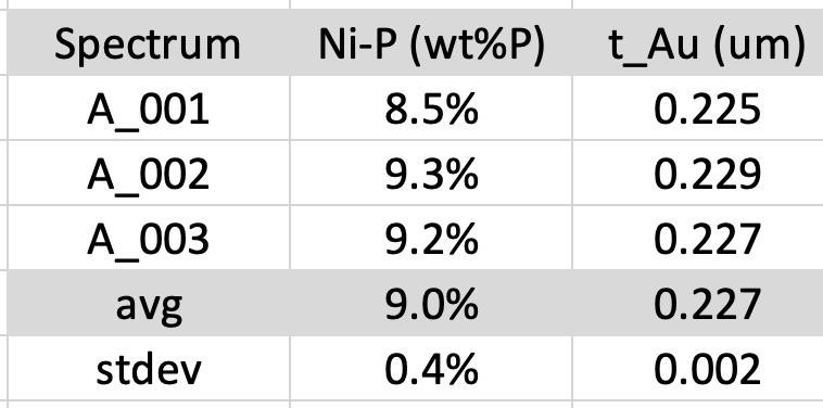
The information from SEM/EDS analysis of an ENIG surface:
- provides the gold plating thickness
- gives wt% P in the EN layer (to a depth of ~ 25 micro-inches)
- provides information about the condition of the nickel grain
boundaries and contamination on the pad surface - is very efficient compared to methods such as microsections
(even though this is also recommended in some cases)