PWB Failure Analysis
Printed Wiring Boards (PWBs) Failure Analysis
SEM Lab’s engineers have experience performing PWB failure analysis beginning in 1988, when Ed Hare, PhD supported construction and failure analysis of PWBs used in shipboard electronics and other DOD systems for Honeywell Marine Systems Division’s Product Analysis Laboratory. SEM Lab, Inc. has performed hundreds of individual PWB failure analyses and has accumulated a significant database of the variety of failure modes and mechanisms involved in PWB failures. Observed failure modes and mechanisms include thermal fatigue of plated-through-hole copper, inner layer separation, crazing & measling, delamination, corrosion, black pad syndrome, conductive anodic filament short circuits, rework damage, and others.
SEM Lab, Inc. also offers PWB design and procurement support services aimed at closing the gap between specification requirements and performance objectives. These services include reliability modeling, power cycle testing, and enhanced coupon analysis.
Some SEM images of failures in printed wiring boards (PWBs) and defects in the PWB surface finish are shown below.
Other device failure analysis information:
PWB Failure Analysis Examples
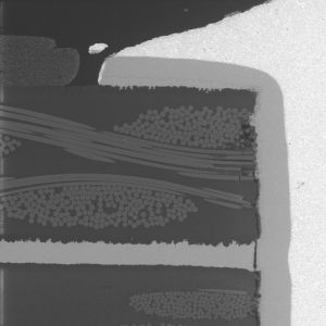
Inner layer separation.
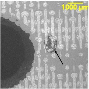
Suspect micro-via.
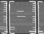
Registration problem.
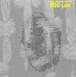
CAF failure planar section.
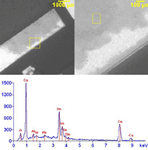
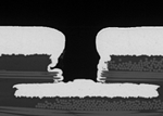
Poor HASL finish.
This is a parallel micro-section of an internal short site in the PWB.

Tin whisker on a flex circuit.