Routine Testing of ENIG Surface Finish
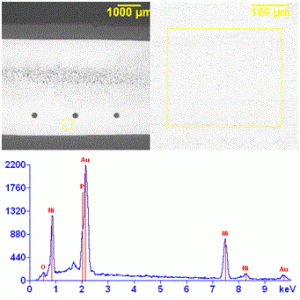
SEM Lab, Inc. supports routine testing of electroless-nickel immersion-gold (ENIG) surface finish on printed wiring boards (PWBs) for quality control objectives. Clients need only send a representative test coupon of ~ 1 inch X 1 inch dimensions. SEM Lab, performs SEM/EDS analysis on the surface pad to acquire a EDS spectrum and examine the pad surface for any anomalous conditions.
A typical EDS spectrum of an ENIG surface is shown in Fig. A. The Au-Ni peak intensity ratio is a measure of the gold thickness. We measure and log this for lot-to-lot comparison with historical data from previous analysis efforts. Similarly, the P-Ni peak intensity ratio is a measure of the weight percentage of phosphorus in the electroless-nickel. Excessive phosphorus levels are an indication of “black pad syndrome” which can cause solderability and reliability problems.
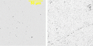
We also characterize the surface condition of the ENIG plating. Fig. B shows two examples of anomalous conditions associated with suspect board lots.
In summary, routine quality control inspection of electroless-nickel immersion-gold surface finish on printed wiring boards can identify anomalous conditions on incoming PWB lots before value added assembly operations with significant avoided costs. The data also serves as a measure of statistical process control for the board surface finish.