PCBA Failure Analysis
Printed Circuit Board Assemblies or PCBA Failure Analysis
The process of PCBA failure analysis depends on the nature of the failure symptoms.
After careful review of all available documentation, followed by examination of the assembly under a stereomicroscope, any anomalies should be documented. Possible anomalies might be suspect solder joints, mechanical damage, discoloration, suspected contamination or corrosion, etc.
Printed wiring board (PWB) related failures generally require cross-section preparation and evaluation to reveal the failure site and root cause of the failure.
Component related failures require either decapsulation or cross-section preparation to reveal the failure site and root cause.
Contamination and corrosion related failures can frequently be characterized without sectioning or decapsulation.
SEM/EDS examination is an important tool used to document the failure site and resolve root cause failures. High resolution images are used to identify the failure mechanism and elemental analysis can reveal chemical or material related factors.
Common causes of PCBA failures include component failures, PTH via opens, electromigration, corrosion, black-pad-syndrome, thermal fatigue, mechanical overstress, and more.
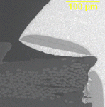
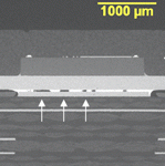
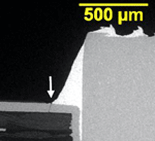
Some failures seen in printed circuit board assemblies (PCBAs) are shown below.
More examples can be found on our examples pages or current on-going examples of PCBA failure analysis can be found on our blog.
Other device failure analysis information:
pcba Failure analysis
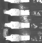
TSOP solder corrosion.
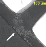
Rework damage of PTH.
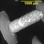
QFN heatsink voids.
Fractured trace.
Un-solderable pins.
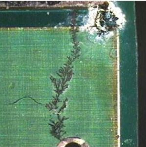
Corrosion shorts signals.
Electromigration short on PCBA.