Miscellaneous Examples
Click on any image to enlarge.
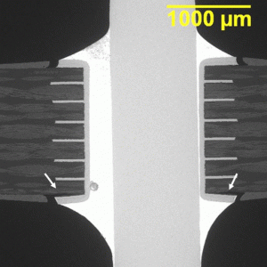
Plated thru hole (PTH) solder joint where the land on the solder side of the board has lifted due to a combination of excessive z-axis expansion of the laminate during wave solder and shrinkage stress in the solder fillet on cool down.
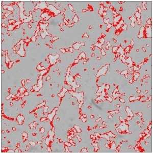
Gold embrittlement of a solder joint. The digitally enhanced "red" pixels correspond to AuSn4 intermetallic compound, lighter areas are Pb, and darker grey is Sn.

