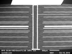
Vias are important features in printed circuit boards as they distribute signals from one layer to another. Occasionally, faulty vias are responsible for electrical failure of PCBAs. This post illustrates a variety of printed wiring board vias and some of the defect conditions we have observed that are associated with vias.
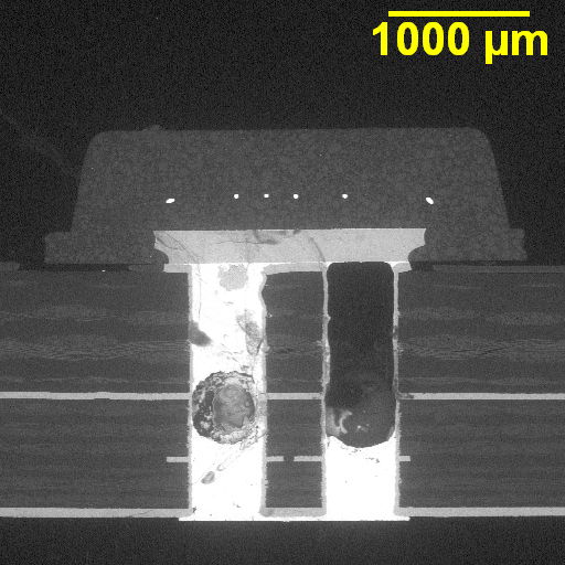
These are thermal PTH-vias associated with a QFN device. The vias are intended to be solder filled, but the solder is nearly absent on one of these two vias, which defeats the purpose of heat conduction away from the device.
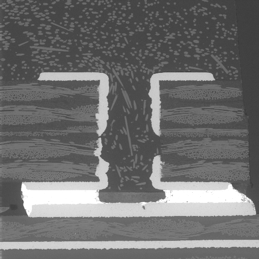
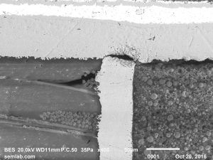
This is a polymer filled PTH-via that exhibited a plating problem. The printed circuit board is a QFN device substrate, where an open circuit condition was attributed to the defective plating.
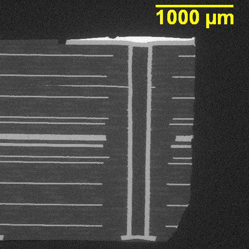
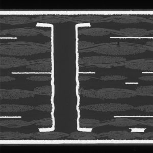
This is a high aspect ratio polymer filled and capped PTH-via that exhibited excellent fill density and copper thickness in the hole.
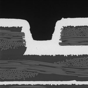
This is a high aspect ratio polymer filled and capped PTH-via that exhibited excellent fill density but showed insufficient copper thickness in the central region of the holes.
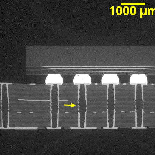
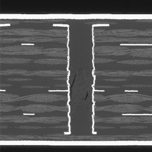
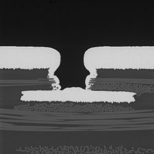
This is a high aspect ratio polymer filled and capped PTH-via that exhibited excellent fill density and copper thickness in the hole (left). However, there was a weakness associated with copper adhesion of the cap to the plated edge of the hole that cause open circuits post reflow soldering (right).
More examples can be found here: