Thermal Cycling Fatigue of a Chip Resistor Solder Joint
A physics-based narrative of damage initiation, crack propagation, and final failure supported by microstructural evidence.
January 30 2026
Ed Hare, SEM Lab. Inc.
1. Introduction
This document describes the physical sequence of events that occur in a SN63 solder joint supporting a chip resistor during accelerated thermal cycling. The narrative integrates mechanics-based fatigue modeling with direct metallographic evidence, demonstrating how cyclic thermo-mechanical strain accumulates and ultimately produces electrical failure.
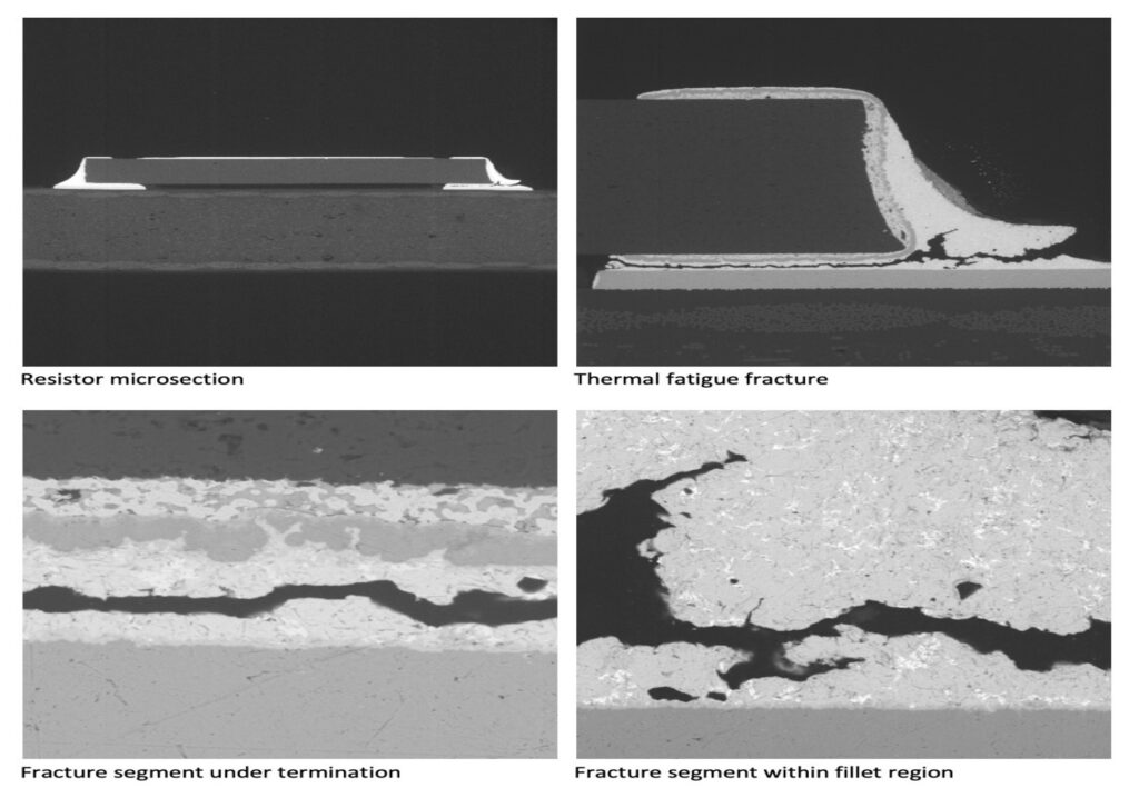
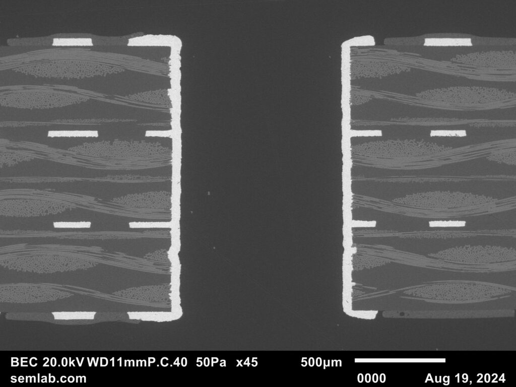
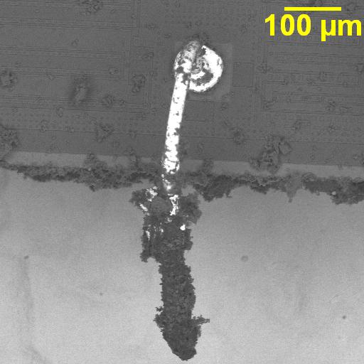
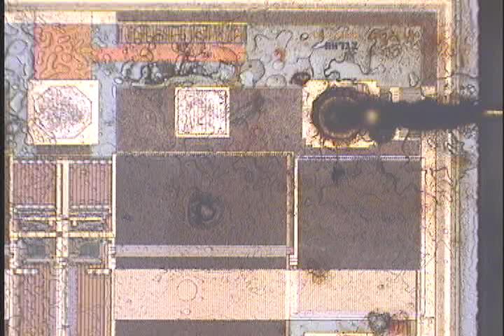
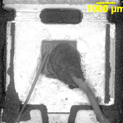
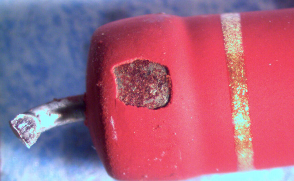
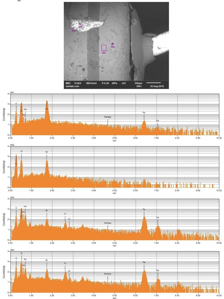
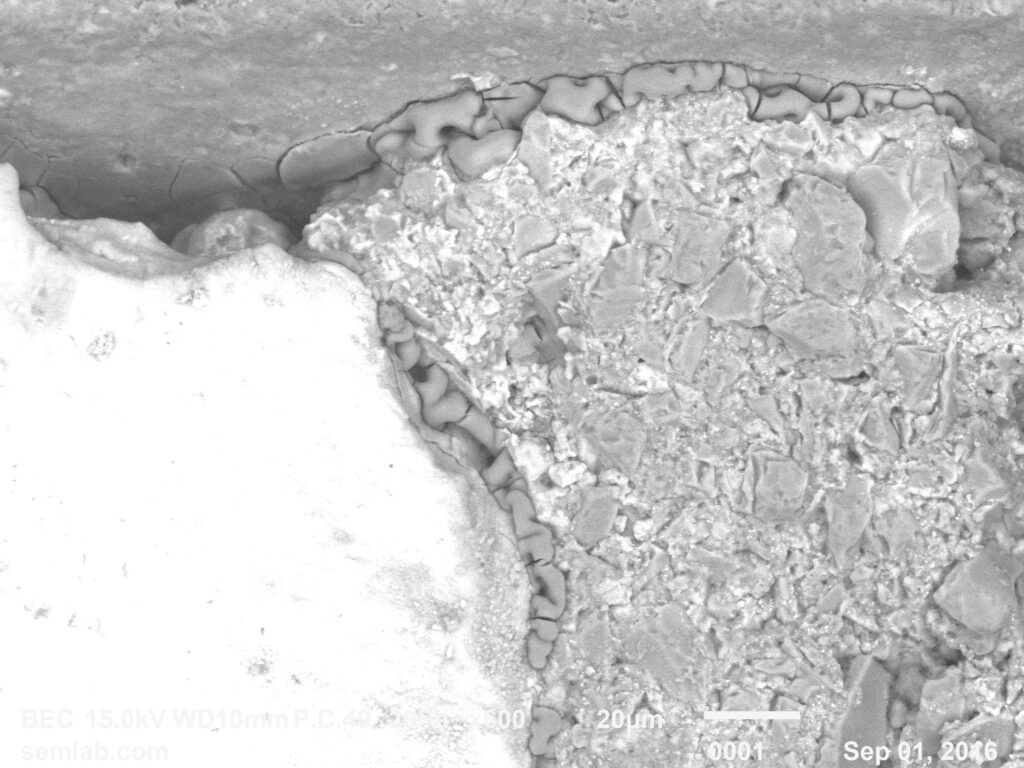
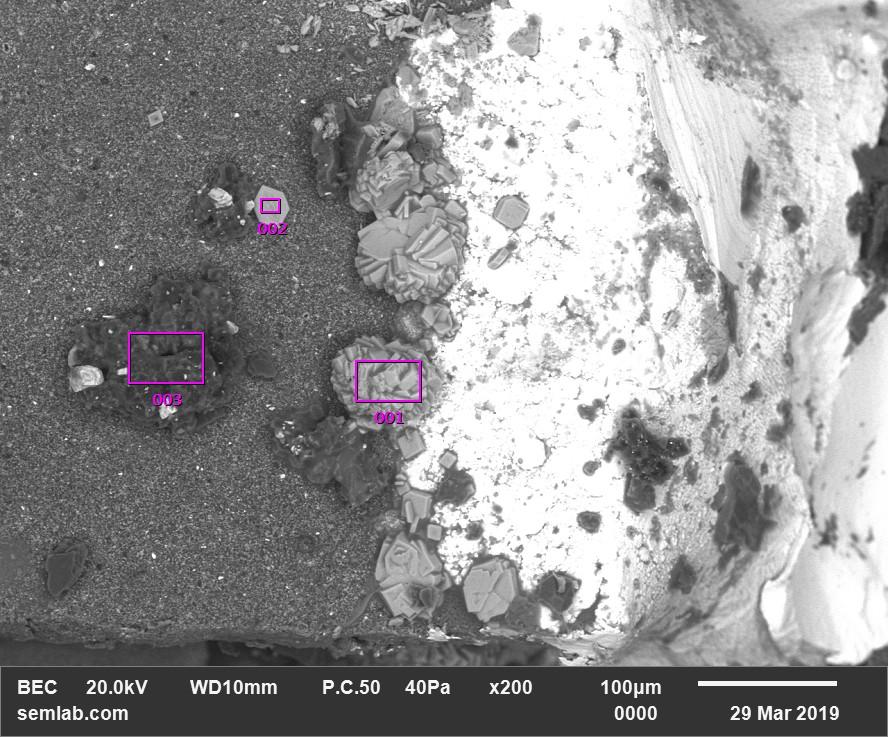
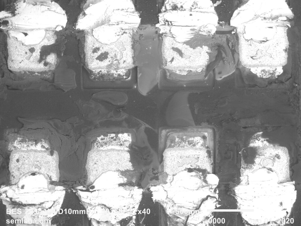
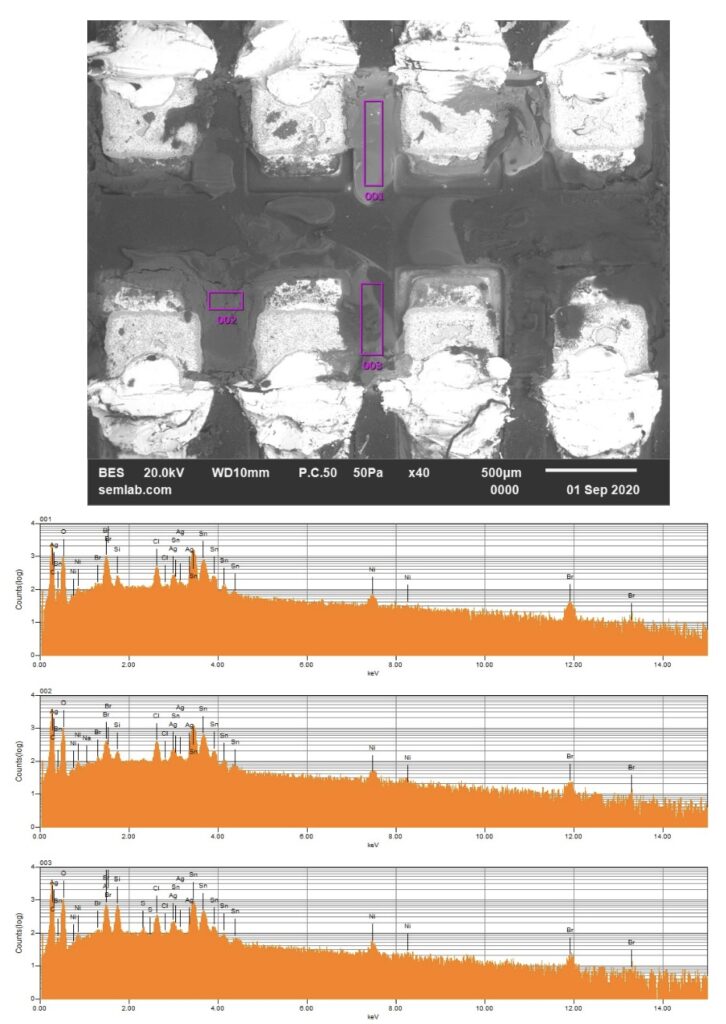
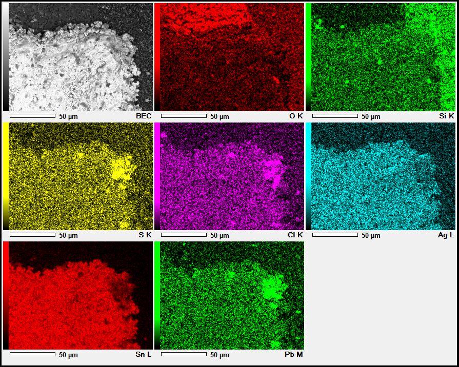
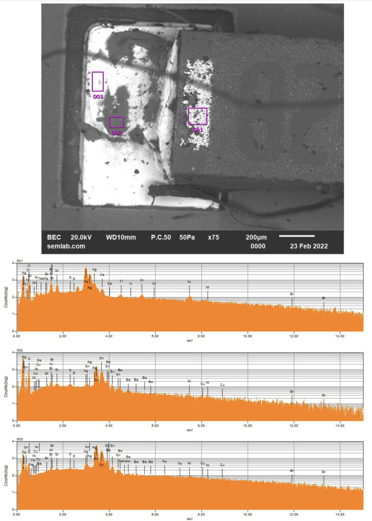
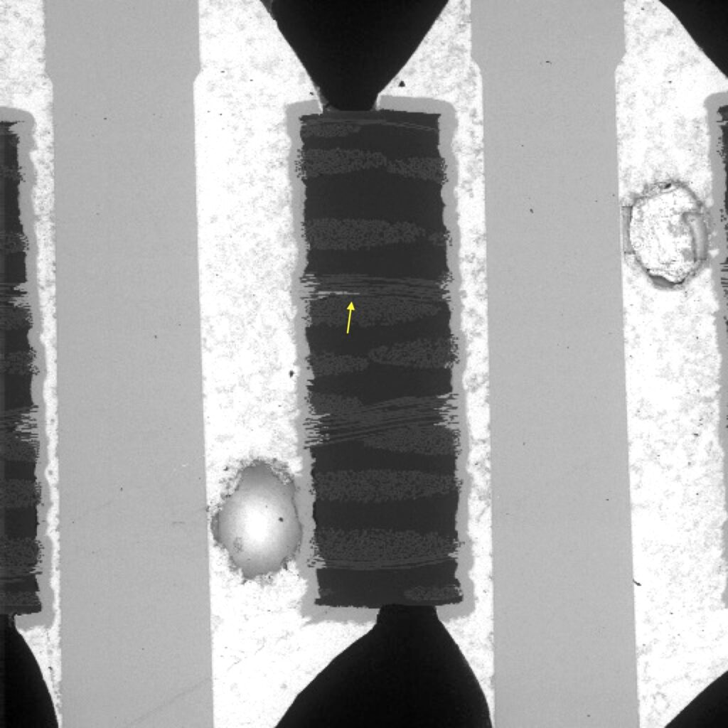
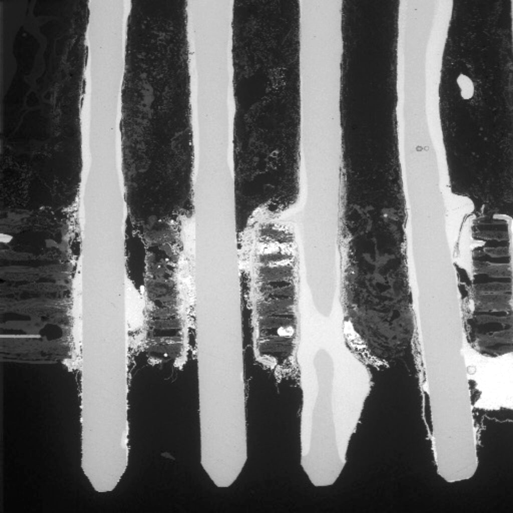
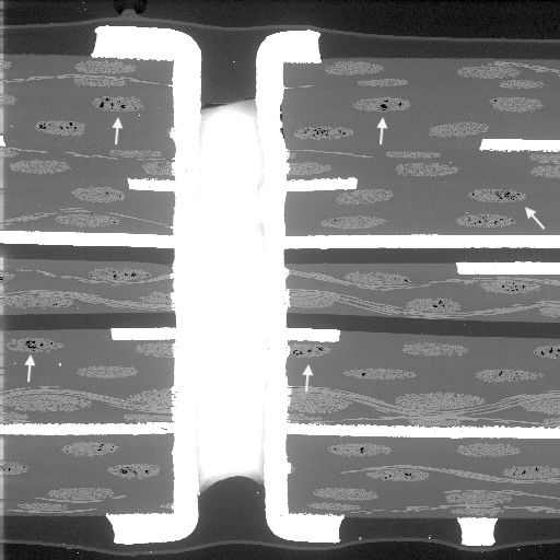
Figure 1. Cross-sectional SEM micrographs of a chip resistor solder joint: (top-left) as-assembled microsection; (top-right) global thermal fatigue fracture; (bottom-left) subsurface crack beneath termination; (bottom-right) advanced fracture within fillet.
2. As-Assembled Condition: Geometry-Driven Strain Amplification
The as-assembled solder joint exhibits low standoff height and sharp geometric transitions at the termination edges. This geometry produces a high strain amplification factor during thermal cycling. Even under nominal workmanship conditions, the mismatch in coefficients of thermal expansion between the ceramic component, FR-4 PCB, and SN63 solder results in immediate elastic–plastic deformation during the first thermal excursion.
3. Early Cycling: Stress Relaxation with Permanent Damage
During the high-temperature dwell portion of the thermal cycle, solder stress relaxes via creep. While peak stress decreases, plastic strain and microstructural damage are retained. Dislocation motion and grain boundary sliding irreversibly alter the solder microstructure, establishing the conditions for fatigue crack nucleation.
4. Crack Initiation Beneath the Termination
Crack initiation occurs preferentially beneath the component termination, where constraint and shear strain are highest. At this stage, cracks are typically subsurface and electrically benign, explaining why early-life damage is rarely detected by functional testing. This regime corresponds to the low-cycle failure tail observed in fatigue life distributions.
5. Stable Crack Propagation Driven by Inelastic Energy
With continued cycling, the crack propagates incrementally under the influence of cyclic inelastic strain energy. Each thermal cycle deposits additional plastic work at the crack tip, resulting in stable, energy-controlled growth along the solder–IMC interface and adjacent solder matrix.
6. Final Failure: Ligament Overload and Electrical Open
As the effective load-bearing area diminishes, local strain intensifies in the remaining solder ligament. Crack growth accelerates rapidly, culminating in complete separation of the joint. Electrical failure often appears sudden, although it is the result of damage accumulated over hundreds of prior cycles.
7. Modelling
A. First power-up: elastic–plastic strain sets in
The very first thermal excursion from −40 °C toward 105 °C immediately imposes differential expansion between:
- the FR-4 PCB (CTE ≈ 15 ppm/°C),
- the 0603 ceramic resistor (≈ 6 ppm/°C),
- and the SN63 solder joint (≈ 23 ppm/°C).
Because the joint has a high geometric amplification factor (L/2h ≈ 15), the global CTE mismatch is converted into a large local shear strain. The total shear strain range is already ~3.9% in the very first cycle. That is well beyond purely elastic behavior — the joint yields almost immediately.
B. Hot dwell: stress relaxes, damage does not
At the 105 °C hot dwell, the solder undergoes time-dependent creep. The peak shear stress (≈ 34 MPa) partially relaxes, falling to about 59% of peak during the dwell.
This often creates a false sense of safety — but physically:
- stress relaxation does not undo plastic strain,
- it locks in permanent microstructural damage.
Our retention metric (W_relax ≈ 0.63) shows that a large fraction of the stress cycle remains fatigue-relevant even after relaxation. In other words, the joint never “resets.”
C. Cooling reversal: strain reverses before structure recovers
As the assembly cools back toward −40 °C, the direction of shear reverses:
- previously elongated regions are now compressed,
- previously compressed regions are now elongated.
However, the solder’s microstructure has already evolved during the hot dwell:
- dislocation density has increased,
- grain boundaries have slid,
This produces a closed hysteresis loop — the area of which is your inelastic energy proxy (W ≈ 0.79 MPa per cycle). That area is irreversible damage.
D. Early micro-crack nucleation (order of N₁ ≈ 75 cycles)
Because strain is highest at geometric discontinuities, the first microscopic cracks form:
- at the solder-to-termination interface,
- typically near the toe of the joint where constraint is highest.
This aligns with the N₁ life (~76 cycles) predicted by the Darveaux framework:
a small percentage of joints will already have a physically detectable crack very early in life.
At this stage:
- the joint is still electrically continuous,
- resistance is unchanged,
- visual inspection usually shows nothing.
But mechanically, the failure process has started.
E. Stable crack propagation driven by cyclic plastic work
With continued cycling:
- each hysteresis loop deposits more inelastic energy at the crack tip,
- the crack grows incrementally during each cycle,
- growth accelerates slightly as the effective load-bearing area shrinks.
This is the Darveaux propagation regime — energy-controlled, not stress-controlled.
The crack advances roughly along the solder–IMC interface or through the solder near that interface, depending on local microstructure.
Importantly:
- stress relaxation does not stop this phase,
- it only redistributes where the damage accumulates.
F. Approach to median failure (N₅₀ ≈ 750 cycles)
By the time ~50% of joints have failed:
- the dominant crack has traversed most of the effective joint width,
- remaining ligaments carry increasing local strain,
- stiffness drops measurably.
Electrical opens may appear intermittently first (thermal-dependent opens), then permanently. This corresponds well to the Darveaux N₅₀ ≈ 759 cycles, which is the most physically grounded metric here because it is tied directly to dissipated energy.
G. Final separation: rapid mechanical collapse
Once the crack reaches a critical length:
- only a small solder ligament remains,
- local strain skyrockets,
- fracture completes in just a few additional cycles.
The end state is a classic fatigue-separated solder joint, often with:
- a relatively flat crack face,
- IMC exposed along part of the fracture,
- minimal bulk solder necking (because creep already relieved much of the peak stress earlier).
8. Conclusions
The combined modeling and microstructural evidence demonstrates that solder joint thermal fatigue is a progressive, geometry-driven process governed by cyclic plastic strain and inelastic energy dissipation. The provided images directly validate the predicted crack initiation sites and propagation paths, transforming abstract fatigue metrics into observable physical phenomena.