Residual Molding Compound After Decapsulation
… as an Indicator of Excessive Current Flow and Joule Heating
Ed Hare – SEM Lab, Inc.
Introduction
Residual molding compound is a critical indicator of failure mode in the failure analysis of electronic components such as PMICs, SOTs, diodes, etc. This article explores how the presence of residual molding compound can signal excessive current flow, leading to charred molding compound due to joule heating. Understanding the correlation between residual molding compound and electrical overstress is an essential tool for diagnosing over current failures in electronic devices.
Background
Molding compounds are used to encapsulate semiconductor devices to protect them from environmental factors and mechanical stress. However, during the failure of electronic components, the molding compound can thermally degrade, leaving behind residual charred material after chemical decapsulation. This degradation is often a result of excessive heating caused by high current flow, known as joule heating.
Residual Molding Compound and Electrical Overstress
The presence of residual molding compound on various parts of a device, such as bond pads, bond wires, and die surfaces, can indicate areas where overheating has occurred. Several job reports have documented the association between residual molding compound and electrical overstress:
**Bond Pads and Die Surface **: Residual molding compound has been observed on bond pads (Fig. A) and the die surface (Fig. B). This suggests that these areas experienced significant heating, leading to the charring of the molding compound.
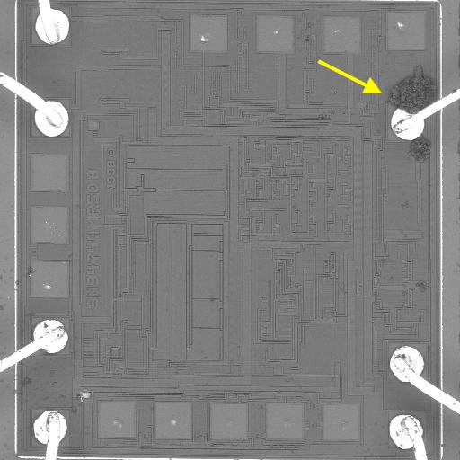
Fig. A – Processor Supervisory Circuit IC, pin-3, power-fail comparator output.
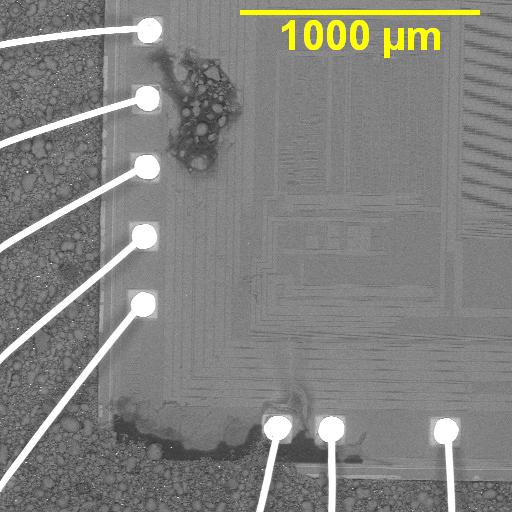
Fig. B – Single-Chip Microcomputer.
**Bond Wires**: residual molding compound on a bond wire serves as an indicator of excessive current cause overheating that is typically centered on the mid-span region of the bond wire, because the bonded ends of the wire are heat sunk and therefore cooler.
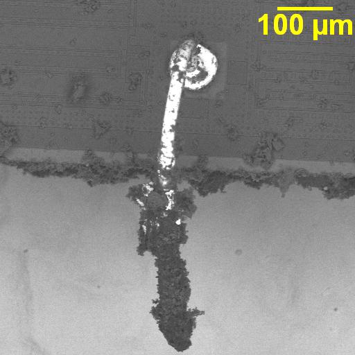
Fig. C – Voltage Regulator, TO-92 package, V_in bond wire.
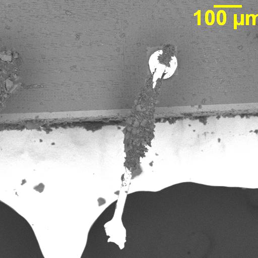
Fig. D – Voltage Regulator, TO-92 package, V_in bond wire encrusted in residual molding compound.
Additional Case Studies
Some additional cases provide examples of how residual molding compound can be used to diagnose electrical overstress:
– **Case 1**: residual molding compound on the die surface indicated a hot spot where the molding compound was charred. This charring made the residual molding compound resistant to the decapsulant, highlighting the severity of the overheating.
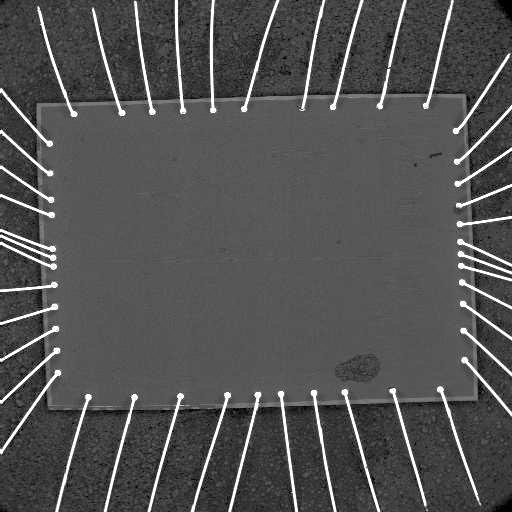
Fig. E – 8-bit Flash Microcontroller, associated with pin-32, an address signal.
– **Case 2**: Residual molding compound on the die surface suggested that the area had over-heated and carbonized the encapsulant resin, providing clear evidence of electrical overstress.
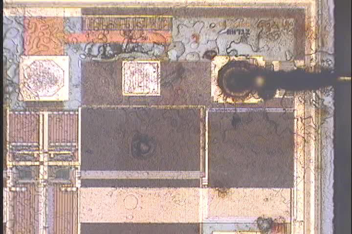
Fig. F – Dual SPDT Switch, optical image of residual molding compound on V+ bond wire.
– **Case 3**: residual molding compound adhered to a MOSFET device centered on the source wire bond and associated die region.
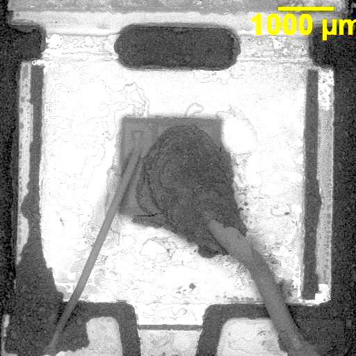
Fig. G – MOSFET device, residual molding compound at source wire bond and associated die region.
Conclusion
Residual molding compound is a valuable indicator of electrical overstress in electronic components. Its presence on bond pads, bond wires, and die surfaces suggests that these areas experienced excessive heating due to high current flow. By understanding the correlation between residual molding compound and electrical overstress, engineers can diagnose failures more accurately and implement measures to prevent similar issues in the future. Our future efforts include thermal modelling to potentially provide pulse width estimates based on estimated volume of residual molding compound.