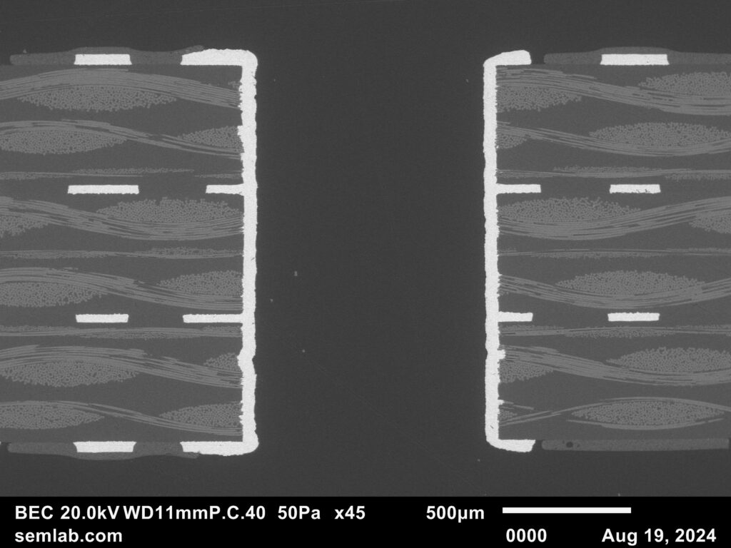
We can use a BSE SEM image of a PWB microsection like this …
… and generate auto feature measurements like this in under a second.
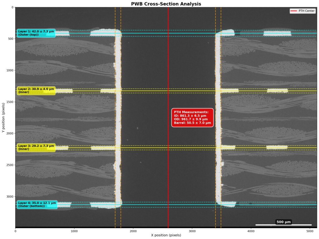
And with a report like this …
# PWB Cross-Section Analysis Report
## Analysis Metadata
– **Report Generated:** 2025-11-12 11:04:20
– **Original Image:** NNNNNN_1.jpg
– **Magnification:** 45x
– **Scale:** 0.53542 µm/pixel
– **Image Dimensions:** 5120 x 3840 pixels (W x H)
– **Copper Coverage:** 5.6%
– **Analysis Method:** Pure Computer Vision
—
## Layer Analysis
| Layer | Y-Centerline (px) | Thickness (px) | Thickness (µm) | Std Dev (µm) | Notes |
|——-|——————-|—————-|—————-|—————|——-|
| 1 | 412 | 78.46 | 42.01 | 7.33 | Outer (top) |
| 2 | 1324 | 57.76 | 30.92 | 4.62 | Inner |
| 3 | 2226 | 54.56 | 29.21 | 7.29 | Inner |
| 4 | 3129 | 65.29 | 34.96 | 12.08 | Outer (bottom) |
## Dielectric Spacing
| Between Layers | Thickness (px) | Thickness (µm) |
|—————-|—————-|—————-|
| Layer 1 to 2 | 831 | 444.93 |
| Layer 2 to 3 | 834 | 446.54 |
| Layer 3 to 4 | 827 | 442.79 |
## PTH Geometry
| Measurement | Value (px) | Value (µm) | Std Dev (µm) |
|————————–|————|————|—————|
| Inner Diameter (ID) | 1608.6 | 861.28 | 6.50 |
| Outer Diameter (OD) | 1796.2 | 961.71 | 9.85 |
| Barrel Copper Thickness | 94.3 | 50.51 | 7.00 |
| Left Barrel | 98.2 | 52.57 | 8.67 |
| Right Barrel | 90.5 | 48.45 | 4.80 |
## Summary
– **Total layers detected:** 4
– **Outer layer thickness (avg):** 38.48 µm
– **Inner layer thickness (avg):** 30.07 µm
– **Average dielectric spacing:** 830.7 px (444.76 µm)
Contact ehare@semlab.com if you are interested in this type of tool for data collection.