SLI_Insight: How I Built a Local Expert Assistant for Electronics Failure Analysis
By Ed Hare
Consultant in Electronic Materials, Reliability, and Failure Analysis
⸻
For more than 27 years, I’ve investigated and solved quality and reliability issues across the electronics industry. In that time, I’ve seen the same problems surface again and again—often buried under too much data and too little insight.
That’s why I developed SLI_Insight, a local expert system that mirrors the way I think, work, and solve problems. It’s not just a chatbot. It’s a distilled version of my consulting methodology—integrating decades of technical experience with a structured database of real failure reports, backed by deep AI summarization.
This tool makes my expertise more accessible and more powerful for clients who need real answers, fast.
⸻
What SLI_Insight Does
SLI_Insight is a locally run expert assistant that helps identify failure causes, trace technical patterns, and retrieve key findings from thousands of archived failure analysis reports. It doesn’t rely on cloud APIs or black-box services. Everything stays local, secure, and private.
The system:
✅ Accepts natural-language queries like:
“What causes solder joint fractures on ENIG plated boards?”
✅ Instantly matches those queries to real report tags using a custom keyword index
✅ Uses SQLite to retrieve relevant sections (background, results, conclusions, figures) from prior reports
✅ Uses a local LLaMA 3.2 model to summarize the findings—grounded in real casework
✅ Outputs a clean, timestamped markdown log of the session and final summary
⸻
How I Built It
The core components of SLI_Insight reflect how I approach every consulting problem:
🧠 Knowledge-Driven Search
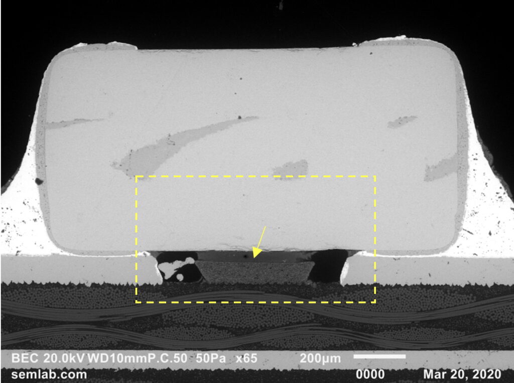
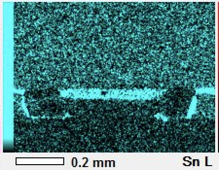
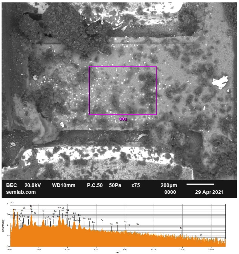
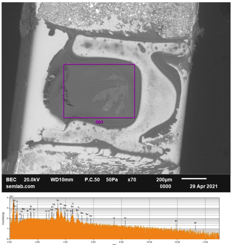
The system uses pre-tagged keywords and job classification data, drawn from thousands of real SEM Lab reports. Instead of relying on vague AI guesses, it retrieves failure analysis content that matches the exact technical terms you care about—cracks, CAF, ENIG corrosion, MLCC knit line failure, and more.
🧰 Structured Retrieval + SQL Logic
Each match triggers SQL queries that pull:
•The original background, results, and conclusions
•Any figure captions and image filenames
•Keywords used in the report
This structured access means I can link a symptom (e.g. “thermal fatigue”) to dozens of real-world case examples in seconds.
🤖 Local Summarization with LLaMA
At the end of each session, SLI_Insight sends relevant text into a locally running LLaMA 3.2 model for expert summarization. Unlike chatbots that “guess” answers, this summary is grounded in actual case data—something no public model can offer.
📝 Everything is Logged and Exported
All interactions are stored in a markdown file, making it easy to build reports, client updates, or technical writeups from any session. The assistant also auto-saves a standalone summary of each session’s key findings.
⸻
Why This Matters for Clients
SLI_Insight isn’t just a clever toy. It’s a force multiplier for my consulting services:
•I can find precedents and patterns in seconds, not hours
•I can trace uncommon failures back to materials, processes, or conditions
•I can deliver findings backed by data—not hunches
In short, I can help your engineering team solve problems faster, with clearer documentation and higher confidence in root cause.
⸻
Interested in Working Together?
If you’re facing yield loss, intermittent failures, or unexplained component damage—and you don’t have months to spare—I can help.
You bring the symptoms and the samples.
I bring the method, the memory, and the insight.
👉 Reach out to start a conversation.
ehare@semlab.com
SEM Lab, Inc.