Failure Analysis and Scanning Electron Microscopy

Call To Action

Call To Action

Failure Analysis and Scanning Electron Microscopy Services

LEARN MORE

425.335.4400      Email

  • SEM Lab, Inc.
  • Services
    • Failure Analysis
    • Electronic Component Failure Analysis
      • F/A of Capacitors
        • Film Capacitors
      • F/A of Resistors
        • Chip Resistor Corrosion
      • F/A of Inductors
      • F/A of Diodes
      • F/A of Transformers
      • F/A of LEDs
      • F/A of ICs
      • F/A of PWBs
      • F/A of BGAs
      • F/A of PCBAs
      • F/A of Medical Devices
      • Identifying Counterfeit Parts
      • PWB Construction Analysis
    • Materials Analysis
      • Solder Joint Analysis
        • Modeling BGA Solder Joints
        • BGA Assembly Verification
        • EDS Data from Sn-Pb Standards
        • Lead Free Solder Analysis
      • Particle Analysis
      • Fiber Analysis
    • X-Ray Inspection
    • FTIR Analysis
      • FTIR of Plastic Parts
    • Scanning Electron Microscopy
    • Microscopy
    • EDS Analysis
      • Thin Film Thickness Measurements
      • EDS Analysis of Polymers
      • EDS Analysis of Alloy Plating
    • Plating Thickness Measurements
    • Quality Control
      • ENIG Quality Control
  • Examples
    • Devices
    • Materials
    • Cross Sections
    • Miscellaneous
  • Request for Quote
  • Papers
    • Intermetallics in Solder Joints
    • Failure Analysis of BGAs
    • Failure Analysis of LEDs
    • Gold Embrittlement of Solder Joints
    • Failure Analysis of PCBAs
    • Diffusion Barrier Plating in Electronics
    • FTIR Analysis
    • Images of Failures in Microelectronics Packaging
    • Failure Analysis of Aluminum Electrolytic Capacitors
    • Solder Joint Analysis
    • BGA Assembly Verification
    • HASL Finish on PWBs
    • PWB Failure Analysis
    • Solder Flux Residue – Part 1
    • Solder Flux Residue – Part 2
  • Blog
  • Contact Us

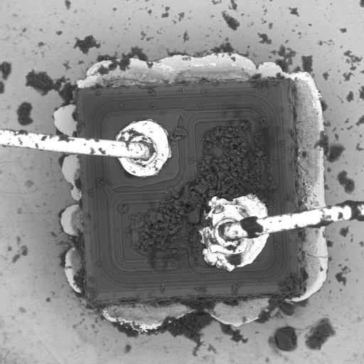
Transistor Failure

Transistor failure caused by electrical overstress damage across most of the emitter region of the die.

Transistor failure caused by electrical overstress damage across most of the emitter region of the die.

Leave a comment

Contact Info

© 2023 SEM Lab Inc. | Privacy Statement | 425-335-4400 | info@semlab.com