Fracture
PCB Pad Cratering
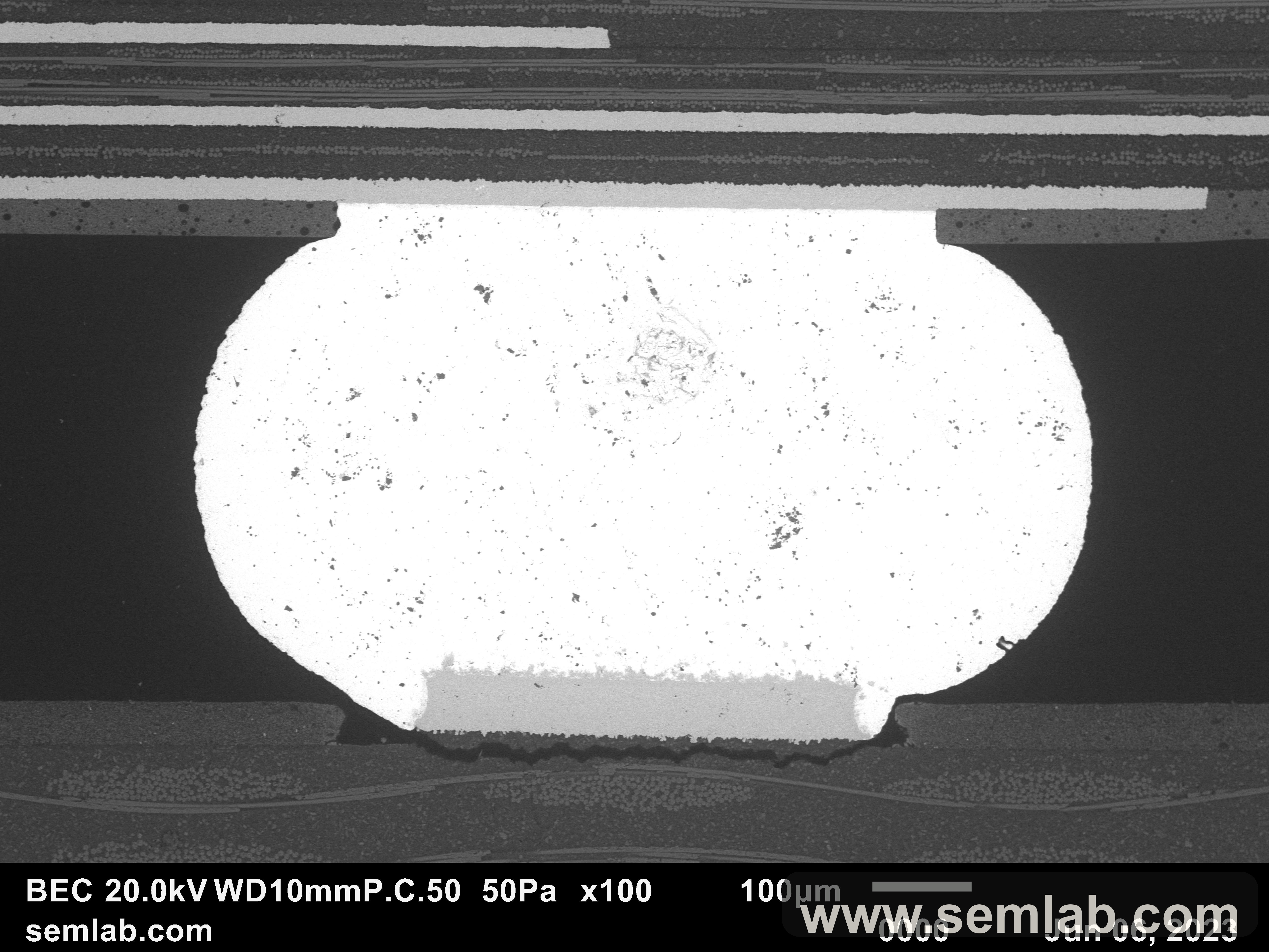
A higher-magnification view of a BGA interconnect showing failure at the ball/PCB pad interface, classified here primarily as PCB pad cratering from board bending.
Interpretation
Why this image matters
This image shows a board-bending-related interconnect failure in a form that is easy to compare with other area-array damage mechanisms.
The report attributed the failures primarily to high strain rate bending of the PCBAs and described the damage as a combination of PCB pad cratering and brittle interfacial fracture.
The primary mechanism here is PCB pad cratering, which makes the image a strong reference for bending-driven damage at the board pad.
fracture
pcb-pad-cratering
bga
board-bending
Use this when
Best comparison value
- Reference: PCB pad cratering in area-array interconnects
- Discussing board-bending damage during handling or test
- Comparing pad cratering to interface fracture and voiding
Related content