Solder Voids
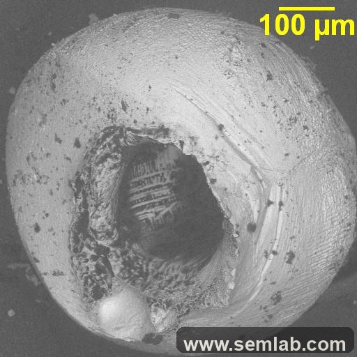
BGA Interface Void
A single large void concentrated at the ball-to-pad interface, showing why void location matters more than raw void presence.
Interpretation
Why this image matters
The void is concentrated at a mechanically and electrically relevant interface rather than appearing as dispersed bulk porosity.
The underlying report noted significant voiding associated with U1 and observed contamination consistent with solder-mask constituents in the broader image set, making the image valuable for process-context discussion as well as morphology.
The failure question here is not simply whether a void exists, but where it sits and what that position means for joint performance.
solder-voids
bga
interface-void
assembly-quality
Use this when
Best comparison value
- Reference: void location versus simple void count
- Discussing BGA pad-interface significance
- Comparing meaningful interface voids to less critical bulk porosity
Related content