Electrical Overstress
IC Die-Level EOS
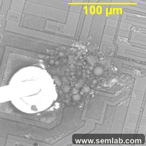
Localized electrical overstress damage in the output region of an integrated-circuit die, with enough surrounding geometry visible to preserve metallization context.
Interpretation
Why this image matters
This image is one of the strongest current SEM Lab examples of die-level electrical overstress because it preserves enough surrounding die geometry to show where the damage sits relative to the output-region metallization.
The underlying report concluded that the devices failed due to EOS damage of one or both outputs, with the visible damage consistent with either an output-to-VCC short-circuit condition or a high transient voltage on the output.
For review, this makes the image especially valuable as a primary-site interpretation reference rather than just a dramatic thermal-aftermath figure.
eos
ic-die
metallization
output-damage
Use this when
Best comparison value
- Reference: die-region EOS versus generic burn damage
- Discussing localized primary electrical damage
- Showing that context around the damaged site still matters
Related content