Case 334 · Public preview
Passivation Defects Can Concentrate Where Wide Metal Buses Increase Interfacial Stress
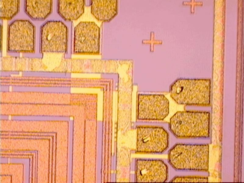
Three bare semiconductor dice contained chipped, missing, and locally delaminated silicon-nitride passivation over portions of their metal buses.
Bright-field optical microscopyDark-field optical microscopyBackscattered-electron SEMEDSDefect-location comparison
What the evidence preview establishes
The defects were most consistent with poor adhesion between the silicon-nitride passivation and the underlying metal buses. Their concentration over wider bus regions indicated that residual or thermal stress likely contributed to separation and chipping.
Why this case matters
Map passivation defects against conductor geometry before assigning them to handling. Interference fringes, retained film flakes, and concentration over wide metal regions can identify an interfacial stress-and-adhesion problem.
Full evidence reserved for MEMBER and STOREThe complete case includes the evidence sequence, four interpreted figures, alternative explanations, limitations, and practical application guidance.