Case 741 · Public preview
A PWB Can Have Both Hidden Interconnect and Visible Solderability Defects
A bare multilayer PWB was submitted for construction analysis before assembly. Both solderable-pad coverage and plated-through-hole inner-layer connections required assessment.
Optical microscopyBSE SEMEDSPTH microsectioningLayer-thickness measurement
What the evidence preview establishes
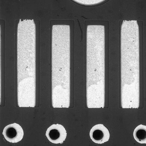
The board was unacceptable for two independent reasons: severe separation at multiple inner-layer-to-PTH connections and incomplete hot-air-solder-leveling (HASL) coverage on mounting pads.
Why this case matters
Inspect solderability finish and hidden PTH connections separately. Acceptable copper thickness does not rescue a separated inner-layer interface, and a visually plated pad may still have inadequate solder coverage.
Full evidence reserved for MEMBER and STOREThe complete case includes the evidence sequence, 4 interpreted figures, alternative explanations, limitations, and practical application guidance.