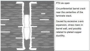
These are some representative solder joint failure modes found in this laboratory that illustrate

* mechanical overload at high strain rate,
* thermal fatigue accelerated by gold embrittlement,
* creep rupture failure

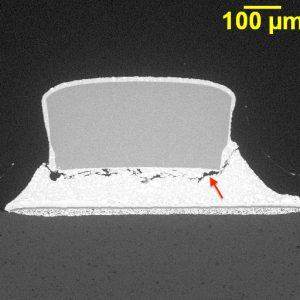
Example 1: This is an SMT thick film resistor solder joint. The solder joint failed in a brittle fracture mode at the interface between the solder and the nickel barrier plating (i.e. brittle interfacial fracture). The analysis results suggested that the resistor failure was most likely caused by mechanical stress (likely in bending) at a high strain rate.

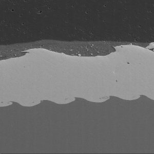
Example 2: This example shows a thermal fatigue fracture. The solder alloy is SN63, the package is a J-lead PMIC, and it is soldered to an alumina substrate. The thermal fatigue fracture showed classic characteristics such as grain boundary separation and propagation through the bulk solder joint. In this case, the failure was accelerated by gold embrittlement of the solder joint (bulk solder joint contained ~ 3 wt% of gold). Fracture is driven by cyclic creep-fatigue damage due to elastic displacement of the leads being converted to time-dependent plastic (creep) strain in the solder joint during thermal cycling. The cyclic strain is due to CTE mismatch between the PMIC and the ceramic substrate.

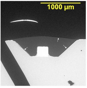
Example 3: This example shows a creep rupture failure of an SMT connector solder joint. The lead that failed was under stress as-soldered. The vertical displacement of the lead after the solder joint fractured is the key feature that suggests this was a creep rupture failure. The elastic strain of the lead is converted to creep strain in the solder joint until it either ruptures or the stress is relieved.

It is important to identify the failure mode accurately in order to formulate appropriate corrective actions.

This is a BSE SEM image of a glass rectifier diode that was chemically decapsulated to remove the glass case.

This is the diode die, which showed two separate breakdown sites that likely occurred simultaneously.

The die fractures are due to thermal shock due to the thermal effect rapid quenching by the surrounding die material immediately after the event.

This type of breakdown is likely due to a fast voltage transient.

BGA warpage can cause a condition called “pad cratering”.

This condition occurs when the assembly cools down below the solidus temperature after reflow soldering and the solder joint is put under tensile loading that exceeds the cohesive strength of the PWB laminate.

The condition often leads to open circuit failures that affect assembly yields.

BGA solder joint microsections are useful for evaluating microstructure, interfacial intermetallic layer thickness, voids, and other conditions. The example below shows a nominal BGA solder joint on 0.8 mm pitch.

In addition, the geometry of the solder joint can provide useful data such as deviation from the nominal condition and the magnitude of residual warpage.

For the above example, i.e. nominal BGA solder joint geometry, the parameters of the solder joint geometry are …

Nominal SJ Height (mm) = 0.25
PWB Pad Dia. (mm) = 0.50
BGA Pad Dia. (mm) = 0.40
h2 (mm) = 0.10
h3 (mm) = 0.15
r1 (mm) = 0.30
Solder Vol. (mm^3) = 0.0661

In summary, there is much to be learned from BGA solder joint microsections.

MICROSECTIONS

The terms microsections and cross-sections and metallography all refer to essentially the same process, which has been in use for a very long time.  This metallurgist was first involved in preparation of metallurgical sections in 1979 while working as a Project Engineer for Northwest Technical Industries, which is now PA&E’s Bonded Metals Division.  Metallographic cross-sections such as the one shown in Fig. A were prepared using standard metallographic practices to document the “wave pattern” and other features of the explosively bonded material.

Explosively bonded metals
Fig. A – Metallographic cross-section of explosively bonded aluminum-steel material. (Sample courtesy of High Energy Metals, Sequim, WA)

The same standard metallographic practices are used to microsection electronic components, printed wiring boards, solder joints, etc., which are typically combinations of metallic, ceramic, and polymeric materials.  Some examples are shown below.

BSE SEM image of a microsection of an LED
BSE SEM image of a microsection of an LED.
Microsection of a multilayer printed circuit board
Microsection of a multilayer printed circuit board.
Microsection of a solder joint showing thermal fatigue failure
Microsection of a solder joint showing thermal fatigue failure.

Preparation of microsections is more difficult for combinations of soft materials (metal & polymers) and hard materials (ceramic & semiconductors) because the soft materials polish at a faster rate than the harder materials.  Nevertheless, it is worth the effort because root cause failure analysis often requires examination of microscopic material details such as microstructure, grain size, porosity, deformation, etc. that would be difficult or impossible to examine using other techniques.  Measurements of solder joint height in microsections can be used to calculate the degree of thermal-mechanical warpage in a BGA assembly as illustrated below.

BGA warpage - How much is too much?
Calculating warpage based on measurements from BGA microsections.

In the previous two decades, black-pad-syndrome was a leading cause of intermittent BGA electrical failure. In 2018, this seems to have been replaced by head-in-pillow defect. Both of these conditions generally require microsection analysis for a conclusive diagnosis as non-destructive techniques mostly fail to identify a problem. Here are some examples of head-in-pillow defect analyzed at SEM Lab, Inc.

Head-in-pillow defect at ball-A3

Head-in-pillow defect at ball-B5

This condition is primarily caused by thermal-mechanical warpage of the BGA during the solder reflow process. Some corrective action recommendations can be found in [1].

[1] SMT Troubleshooting Guide, “BGA Head-on-Pillow”, www.alpha.cooksonelectronics.com, Issued 10/08, p. 17.

An IR LED was submitted for failure analysis. The LED had failed during process validation testing.

These are optical images of the IR LED documenting the results of external examination.

This image shows a microsection just after grinding into the cup. The angle of the gold bond wire near the wire bond appeared to be anomalous.

The open-circuit failure was caused by bond wire fracture that occurred just above the wire bond.

This is a higher magnification image of the fractured bond wire.

The failure was most likely caused by thermal (or possibly mechanical) stress putting tension on the bond wire, and there may have also been some damage to the bond wire as a result of the original wire bonding process during fabrication of the LED.

A Dual Operational Amplifier IC was submitted for failure analysis.

This is an optical image of the device.

This is a BSE SEM image of the device after chemical decapsulation.

This is a higher magnification image of the device die.

This is electrical over-stress damage associated with an output, OUT2.

This is an elemental dot map that shows aluminum exposed through the passivation layer in the damaged areas.

The analysis results suggested that the device failed on OUT2 due to a high voltage transient event on the OUT2 signal.